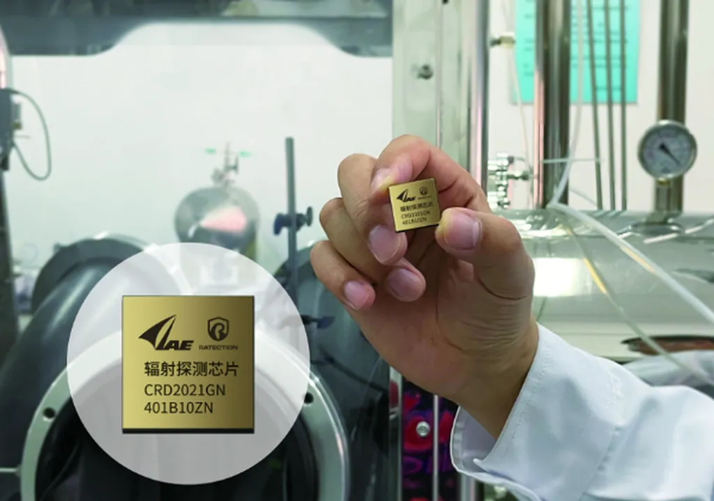
In the realm of occupational safety, particularly in the energy sector, the ability to monitor radiation exposure accurately and efficiently is paramount. A recent breakthrough in this area comes from researchers at the China Institute of Atomic Energy, who have developed a low-power, high-sensitivity CMOS integrated circuit tailored for personal dosimeters. This innovation, detailed in the journal *Atomic Energy Science and Technology*, could significantly enhance the reliability and portability of radiation monitoring devices.
The team, led by Dr. Liu Zhan, has designed a front-end CMOS chip circuit specifically for boron nitride (BN) neutron detectors. Boron nitride, a fourth-generation wide band gap semiconductor, boasts exceptionally low room-temperature leakage current, eliminating the need for cryogenic cooling. This feature not only simplifies the detection process but also makes the technology more accessible for field use.
“Our goal was to create a circuit that could reliably convert neutron signals into charge signals without the need for additional conversion layers,” explained Dr. Liu. “This streamlining not only reduces the complexity of the detection chain but also enhances the overall efficiency of the dosimeter.”
The circuit’s architecture is composed of four critical modules: a low-noise charge-sensitive preamplifier (CSA), a CR-RC shaping filter, a precision reference current source, and a hysteresis voltage discriminator. The CSA employs a gain bootstrapping structure with an NMOS input, dynamically stabilizing the gate-source voltage of the input transistor to enhance noise performance. This configuration achieves a transimpedance gain of 5 mV/fC while maintaining a low input-referred noise floor.
One of the key innovations in this design is the dynamically adjustable feedback resistor network, which addresses baseline drift induced by detector leakage. This adaptive design ensures the circuit remains linear across a wide range of radiation fluxes, with an integral nonlinearity of less than 1%.
Fabricated in SMIC 55 nm CMOS technology, the circuit operates at a 1.2 V supply voltage, achieving a single-channel power consumption of 0.22 mW. Post-layout simulations demonstrate an equivalent noise charge (ENC) of 3e− at zero detector capacitance, making it suitable for detectors with up to 10 pF capacitance.
The shaping filter’s 5 μs peaking time optimizes the signal-to-noise ratio for typical neutron-induced charge pulses, ensuring reliable pulse counting in noisy environments. This design exemplifies the integration of advanced semiconductor technology with nuclear detection principles, offering a compact, low-power solution for next-generation personal dosimetry systems.
The implications of this research are far-reaching, particularly for the energy sector. As nuclear power continues to play a crucial role in global energy production, the need for reliable and portable radiation monitoring devices becomes ever more critical. This innovation could pave the way for more efficient and accurate personal dosimeters, enhancing safety protocols and operational efficiency in nuclear facilities.
Dr. Liu and his team’s work sets a new benchmark for front-end stability in radiation detection applications, particularly for portable devices requiring long-term operation on battery power. As the energy sector continues to evolve, such advancements in technology will be instrumental in ensuring the safety and efficiency of nuclear operations.
Published in the journal *Atomic Energy Science and Technology*, this research represents a significant step forward in the field of radiation detection, offering a glimpse into the future of personal dosimetry systems. The dynamically adaptive feedback mechanism developed by Dr. Liu and his colleagues not only enhances the reliability of these devices but also underscores the potential for further innovations in this critical area of safety technology.