In the high-stakes world of semiconductor manufacturing, where even the tiniest impurities can spell disaster, a new study is shedding light on a crucial process that could significantly boost production yields and efficiency. Published in the journal *Applied Sciences* (translated from *Applied Sciences*), the research, led by Stephen Sammut of the Institute of Engineering and Transport at the Malta College of Arts, Science and Technology, delves into the intricate world of plasma cleaning, a vital yet often overlooked aspect of semiconductor packaging.
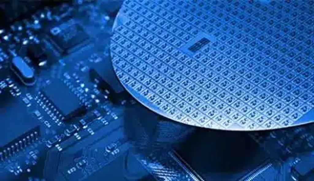
Semiconductor devices are the backbone of modern electronics, powering everything from smartphones to renewable energy systems. At the heart of these devices lies the lead frame, a critical component that provides mechanical support and electrical connections for the silicon dies. However, impurities such as oxides and organic matter on the lead frame’s surface can wreak havoc on the manufacturing process, leading to reduced yields and increased costs.
Plasma cleaning, a non-contact, damage-free method, has emerged as a game-changer in this arena. By generating reactive species like oxygen radicals and hydrogen ions, plasma systems can efficiently remove contaminants without the need for harsh chemicals. “Plasma cleaning offers significant advantages over conventional wet chemical processes,” Sammut explains. “It’s precise, efficient, and environmentally friendly, making it an attractive option for modern semiconductor manufacturing.”
The study provides a comprehensive overview of plasma cleaning processes, with a particular focus on lead frame cleaning. It explores the fundamental physics behind plasma generation, the design of plasma systems, and the composition of the plasma medium. One of the key aspects of the research is its comparative analysis of different plasma systems, including direct current, dielectric barrier discharge, radio frequency, and microwave-based systems.
Sammut and his team also delve into the role of non-reactive species like argon in sputtering processes. Sputtering, a physical process driven by momentum transfer, involves the ejection of individual atoms from a target surface due to the impact of energetic ions. “By understanding the underlying physics, we can optimize plasma cleaning processes to achieve better results,” Sammut notes.
The research also addresses critical parameters affecting plasma cleaning performance, such as gas chemistry, power input, pressure regulation, and substrate handling techniques. By providing a concise yet comprehensive resource, the study aims to equip technical personnel with the essential knowledge required to make informed decisions about plasma cleaning technologies.
The implications of this research extend beyond the semiconductor industry. As the world shifts towards renewable energy, the demand for advanced semiconductor devices is set to soar. Efficient and environmentally friendly manufacturing processes like plasma cleaning will play a pivotal role in meeting this demand.
Moreover, the study’s findings could pave the way for future developments in plasma cleaning technologies. As Sammut puts it, “Our research provides a foundation for further exploration and innovation in this field. By understanding the intricacies of plasma cleaning, we can push the boundaries of what’s possible in semiconductor manufacturing.”
In the ever-evolving landscape of energy and technology, this research serves as a reminder of the power of innovation. By harnessing the potential of plasma cleaning, we can not only enhance the efficiency of semiconductor manufacturing but also contribute to a more sustainable and technologically advanced future.