Researchers Zijie Wang, Mazharul M. Islam, and David R. Bowler from King’s College London have recently published a study in the Journal of Physics: Condensed Matter, focusing on the atomic and electronic structures of stacking faults in gallium nitride (GaN) materials. Their work uses density functional theory (DFT) calculations to better understand these defects, which are common in GaN and can significantly impact its properties.
Gallium nitride is a crucial semiconductor material widely used in the energy industry, particularly in power electronics and radio frequency devices. Understanding and controlling defects in GaN can lead to more efficient and reliable energy devices. Stacking faults are planar defects that occur during the growth of GaN crystals, and they can influence the material’s electronic properties.
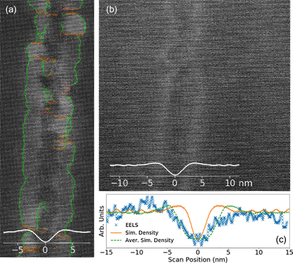
The researchers examined stacking faults in both hexagonal wurtzite (wz) and cubic zincblende (zb) phases of GaN. In the hexagonal phase, they identified three types of intrinsic stacking faults (I1, I2, and I3) and one extrinsic stacking fault (E). In the cubic phase, they found one type each of intrinsic, extrinsic, and twin stacking faults. The study revealed that the I1 stacking fault is the most stable in wz GaN, aligning with experimental observations. For zb GaN, the intrinsic stacking fault is the most dominant planar defect.
The team also investigated how these stacking faults affect the electronic structure of GaN. They discovered that in wz GaN, the bands near the valence band maximum are localized on the gallium-polar side of the stacking fault, while the bands near the conduction band minimum are more on the nitrogen-polar side, though somewhat delocalized. Conversely, in zb GaN, the opposite trend was observed. This behavior is attributed to a redistribution of charge near the interface.
Furthermore, the researchers calculated the band offsets for the stacking faults and found that they are very sensitive to local conditions. However, all stacking faults can be described as type II interfaces, meaning that the presence of a stacking fault reduces the band gap locally. This understanding can help in designing and optimizing GaN-based devices for various energy applications.
In summary, this research provides valuable insights into the atomic and electronic structures of stacking faults in GaN, which can guide efforts to control and utilize these defects for improving the performance of GaN-based energy devices. The study was published in the Journal of Physics: Condensed Matter.
This article is based on research available at arXiv.