Researchers from the Italian Institute of Technology (IIT) in Genoa have made significant strides in the field of semiconductor materials, with potential implications for the energy sector. The team, led by Mehrdad Faraji and including Alexander Schleusener, Sirous Khabbaz Abkenar, Andrea Griesi, Mattia Lizzano, Sudhir Kumar Saini, Aswin V. Asaithambi, Liberato Manna, Matteo Lorenzoni, Mirko Prato, Giorgio Divitini, and Roman Krahne, has developed a novel approach to fabricate two-dimensional (2D) perovskite heterostructures. Their work was recently published in the journal Nature Nanotechnology.
Semiconductor technology is a cornerstone of modern energy systems, from solar panels to energy storage devices. The ability to control and manipulate the flow of charge carriers is crucial for improving the efficiency and performance of these technologies. In this study, the researchers focused on low-dimensional metal halide perovskites, a class of materials that has garnered significant attention for their unique optical and electronic properties.
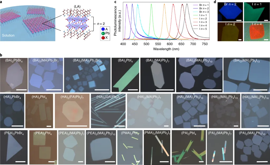
The team demonstrated a versatile one-pot synthesis method to create a variety of 2D perovskite heterostructures. By exploiting sequential crystallization of different 2D perovskites, they were able to design diverse heterostructure architectures, including multiple heterojunctions. This approach allows for precise control over the energy landscape in the plane of the semiconducting lattice, enabling the tailoring of energy barriers and the control of charge carrier flow.
One of the key advantages of this method is its simplicity and flexibility. The researchers were able to achieve high crystalline quality of the heterojunctions, multicolor emission, and optical coupling between different heterostructure regions. These properties are essential for the development of novel optoelectronic devices, where electronic band engineering is crucial.
The practical applications of this research for the energy sector are manifold. For instance, the ability to design and fabricate high-quality heterostructures could lead to more efficient solar cells, as well as improved energy storage devices. The multicolor emission properties could also be harnessed for advanced lighting technologies, contributing to more energy-efficient lighting solutions.
In conclusion, the work of Faraji and his colleagues represents a significant advancement in the field of semiconductor materials. Their versatile and flexible approach to fabricating 2D perovskite heterostructures opens up new avenues for the development of novel optoelectronic devices, with potential benefits for the energy sector. As the researchers themselves note, the design freedom of their method is likely to stimulate further innovation in this exciting field.
This article is based on research available at arXiv.